

The Tau Scaling Law Huawei Proposes End to Geometric Computing Limits
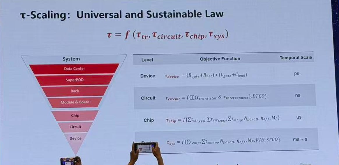
The organization believes that the future of computing will be more reliant on diminishing signal delay throughout the system as opposed to miniaturising transistors.
What Huawei is actually proposing
For many years, the semiconductor sector has depended on technique geometrical scaling (shrinking of the transistor), therefore enabling to increase performance per unit of volume. Semiconductor manufacturers are facing limitations both in terms of physical limitations and cost limitations using this type of technique. As a result, Huawei is developing a paradigm that is based upon creating the architecture of semiconductor devices around time constants (tau), which represents the speed at which signals travel globally throughout a device, circuit, chip, and entire semiconductor system.
On the surface this might sound more conceptual than business logic based, but the reality is that not being able to continue to shrink the size and/or increase the performance of device transistors does not limit technology. Rather, technology can be improved based upon redesigned semiconductor architectures to what they refer to as latency, connectiveness, and optimized systems. According to Huawei, this paradigm can be utilized by them to continue to utilize newer-generation devices and make continued advancements to their business even without having to fully rely on having the latest generation of device fabrication nodes.
Why it matters now
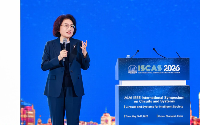
This document does not only offer technical content and fill up space in conference rooms. Huawei implemented this framework at the 2026 IEEE International Symposium on Circuits and Systems in Shanghai. At this time, there is a lot going on globally in terms of chip competition because of export control policies, conformance with supply chain requirements and developing AI-ready hardware.
As well, Huawei has reportedly implemented the use of the tau principle in chip design and mass production for six years, and has purportedly designed 381 chips under this principle. By 2031, they believe they may be able to produce chips with the equivalent of a 1.4 nm class fabrication process.
The design shift behind tau
One interesting thing about Huawei's introduction of tau is that they don't market tau as a singular miracle development. Instead, they describe tau as an engineering optimization across devices and systems (including circuits and chipsets). So rather than attributing performance gains to simply a reduction in physical size, they attribute those gains to a collective increase in the efficiency of the whole stack.
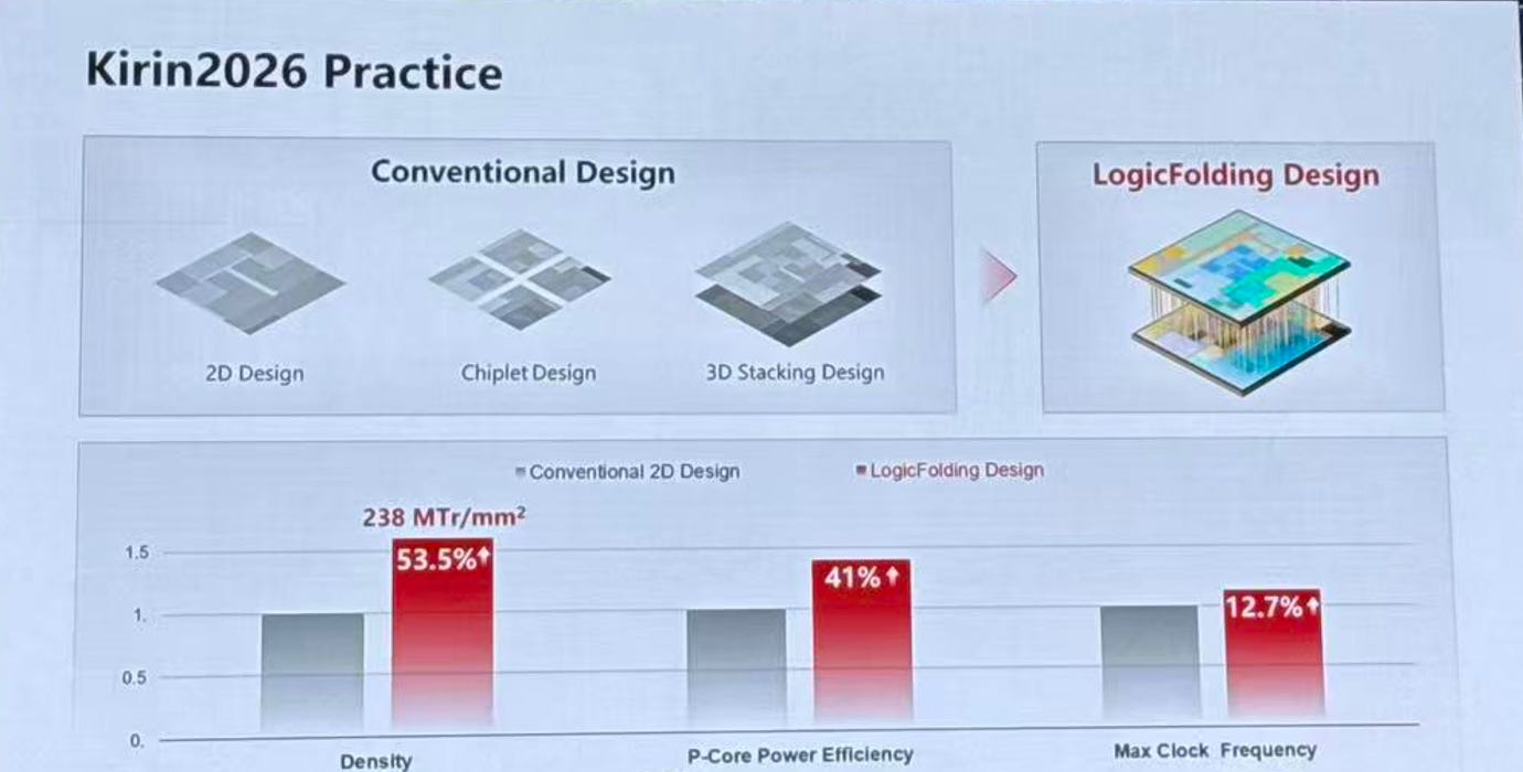
The company's rollout has two engineering names: LogicFolding and UnifiedBus. LogicFolding will reduce the resistive load and capacitive load on signal propagation, while UnifiedBus will reduce the communication latency at the system level. This is also a fundamental engineering advancement with a significant strategic impact. When you compress the time required for information to travel, then you will be able to do more efficient work with the same hardware.
The business stakes
For Huawei, tau encompasses more than scientific achievement; it also encapsulates resilience. To continue achieving better levels of performance by not relying solely on an advanced external manufacturer tooling and suppressing China’s larger goal of developing an independent semiconductor ecosystem through development & R & R&D capabilities.
To develop these approaches, it is important to consider how chip manufacturers are competing today. While historically, having the best technology available was sufficient for achieving top-tier performance in chips, that is no longer the case. With many manufacturers establishing themselves in competitive markets, performance is now determined by who can provide dependable functionality within limited capabilities; those who can work around bottlenecks; and, ultimately, whose overall design is superior. In this context, Huawei is trying to change the conversation from "who has the smallest process node?" to "who has the most effective system-based architecture?"
What this could change for AI and devices
If Huawei's chip-making strategy succeeds on a larger scale, it can impact how future consumer electronics and AI chips are developed as all new workloads require lower latency and better efficiency, particularly with edge computing, AI inference, and mobile devices where energy consumption and speed are essential to their operation as well as their ability to operate simultaneously.
Thus, the tau story represents more than just one company's roadmap for product development; if the industry employs signal timing as a primary design consideration, then the competitive landscape for chipmaking may evolve from just being a volume (size) race to also being defined by architectural considerations.
The cautious read
However, this proposal needs to be proven as the reset of the industry, since Huawei has made claims before and the only way to know if tau survives all aspects of manufacture, cost, performance and mass volume in the market will be by testing these areas with their products.
The logical way to interpret this announcement is as a clear indication of where we are headed as a semiconductor industry due to increasing pressure. As one direction becomes more challenging engineers search for alternate directions. In brief, Huawei is banking that the next advance in technology will not be solely based upon geometry, rather advancing technology through time.
Latest Posts